

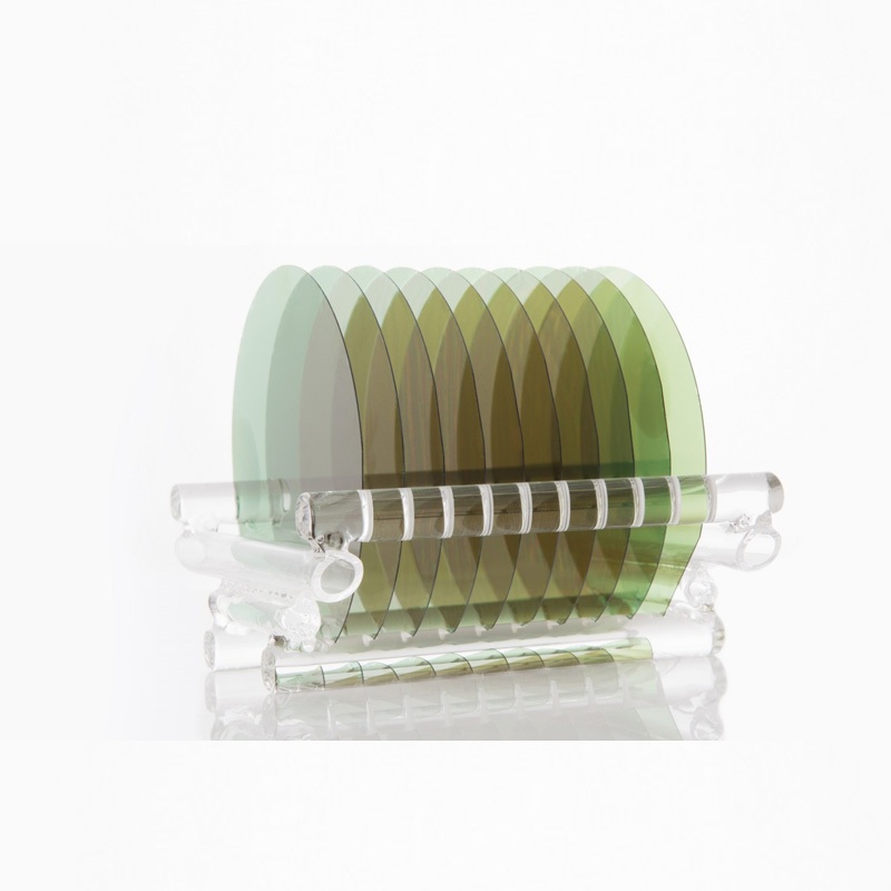
Epitaxial SiC (Silicon Carbide) Wafers
Epitaxial SiC wafers are silicon carbide substrates with an additional SiC layer grown on the surface, typically by CVD (Chemical Vapor Deposition). This epitaxial layer offers superior crystal quality and precisely controlled electrical properties compared to the underlying substrate, making it the material of choice for power semiconductor devices such as MOSFETs and Schottky diodes.
We offer epitaxial SiC wafers in 4, 6, and 8 inch sizes. Custom specifications are available upon request — please contact us to discuss your requirements.
Specifications
|
Grade
|
Production
|
Research
|
Dummy
|
|
|
Diameter
|
50.8mm±0.38mm
|
|||
|
Thickness
|
330um±25um
|
|||
|
Wafer Orientation
|
On axis :<0001>±0.5°for 4H-N/6H-N/4H-SI/6H-SI
Off axis : 4.0°toward<1120>±0.5°for 4H-N/4H-SI
|
|||
|
Micropipe Density
|
≤5cm-2
|
≤15cm-2
|
≤50cm-2
|
|
|
Resistivity
|
4H-N
|
0.015~0.028Ω⋅cm
|
||
|
6H-N
|
0.02~0.1Ω⋅cm
|
|||
|
4/6H-SI
|
>1E5Ω⋅cm
|
(90%)>1E5Ω⋅cm
|
||
|
Primary Flat
|
±5.0°
|
|||
|
Primary Flat Length
|
15.9mm±1.7mm
|
|||
|
Secondary Flat Length
|
8.0mm±1.7mm
|
|||
|
Secondary Flat Orientation
|
Silicon face up : 90 °CW from Prime flat ±5.0°
|
|||
|
Edge exclusion
|
1mm
|
|||
|
TTV/Bow/Warp
|
≤15um/≤25um/≤25um
|
|||
|
Roughness
|
Optical polish Ra ≤1nm on the C-face
CMP Ra≤0.5nm on the Si-face
|
|||
|
Cracks by high intensity light *1
|
None
|
None
|
1 allowed, ≤1mm
|
|
|
Hex plates by high intensity light *2
|
Cumulative area ≤1%
|
Cumulative area ≤1%
|
Cumulative area ≤3%
|
|
|
Polytype areas by high intensity light *2
|
None
|
Cumulative area ≤2%
|
Cumulative area ≤5%
|
|
|
Scratches by high intensity light *2*3
|
3 scratches to 1 x wafer diameter cumulative length
|
5 scratches to 1 x wafer diameter cumulative length
|
8 scratches to 1 x wafer diameter cumulative length
|
|
|
Edge chip
|
None
|
3 allowed, ≤0.5mm each
|
5 allowed, ≤1mm each
|
|
|
Contamination by high intensity light
|
None
|
|||
*1: Defects shall be existed in the edge area ,only defect beyond of the prescribed scope could be considered as reject cause.
*2: Defects shall be existed in the edge area ,only defect beyond of the prescribed scope could be considered as reject cause.
*3: Scratches should be checked on Si face only.
|
Grade
|
Production
|
Research
|
Dummy
|
|
|
Diameter
|
76.2mm±0.38mm
|
|||
|
Thickness
|
350um±25um
|
|||
|
Wafer Orientation
|
On axis :<0001>±0.5°for 4H-SI
Off axis : 4.0°toward<1120>±0.5°for 4H-N |
|||
|
Micropipe Density
|
≤5cm-2
|
≤15cm-2
|
≤50cm-2
|
|
|
Resistivity
|
4H-N
|
0.015~0.028Ω⋅cm
|
||
|
4H-SI
|
>1E5Ω⋅cm
|
(90%)>1E5Ω⋅cm
|
||
|
Primary Flat
|
±5.0°
|
|||
|
Primary Flat Length
|
22.2mm±3.2mm
|
|||
|
Secondary Flat Length
|
11.2mm±1.5mm
|
|||
|
Secondary Flat Orientation
|
Silicon face up : 90 °CW from Prime flat ±5.0°
|
|||
|
Edge exclusion
|
2mm
|
|||
|
TTV/Bow/Warp
|
≤15um/≤25um/≤35um
|
|||
|
Roughness
|
Optical polish Ra ≤1nm on the C-face
CMP Ra≤0.5nm on the Si-face
|
|||
|
Cracks by high intensity light *1
|
None
|
None
|
1 allowed ,≤2mm
|
|
|
Hex plates by high intensity light *2
|
Cumulative area ≤1%
|
Cumulative area ≤1%
|
Cumulative area ≤3%
|
|
|
Polytype areas by high intensity *2 light
|
None
|
Cumulative area ≤2%
|
Cumulative area ≤5%
|
|
|
Scratches by high intensity light *2*3
|
3 scratches to 1 x wafer diameter cumulative length
|
5 scratches to 1 x wafer diameter cumulative length
|
8 scratches to 2 x wafer diameter cumulative length
|
|
|
Edge chip
|
None
|
3 allowed, ≤0.5mm each
|
5 allowed, ≤1mm each
|
|
|
Contamination by high intensity light
|
None
|
|||
*1: Defects shall be existed in the edge area ,only defect beyond of the prescribed scope could be considered as reject cause.
*2: Defects shall be existed in the edge area ,only defect beyond of the prescribed scope could be considered as reject cause.
*3: Scratches should be checked on Si face only.
|
Grade
|
Zero MPD
|
Production
|
Research
|
Dummy
|
|
Diameter
|
100.0mm±0.5mm
|
|||
|
Thickness
|
4H-N
|
350um±25um
|
||
|
4H-SI
|
500um±25um
|
|||
|
Wafer Orientation
|
On axis :<0001>±0.5°for 4H-SI
Off axis : 4.0°toward<1120>±0.5°for 4H-N |
|||
|
Micropipe Density
|
≤1cm-2
|
≤5cm-2
|
≤15cm-2
|
≤50cm-2
|
|
Resistivity 4H-N 4H-SI
|
0.015~0.028Ω⋅cm
|
|||
|
≥1E5Ω⋅cm
|
||||
|
Primary Flat
|
±5.0°
|
|||
|
Primary Flat Length
|
32.5mm±2.0mm
|
|||
|
Secondary Flat Length
|
18.0mm±2.0mm
|
|||
|
Secondary Flat Orientation
|
Silicon face up : 90 °CW from Prime flat ±5.0°
|
|||
|
Edge exclusion
|
3mm
|
|||
|
TTV/Bow/Warp
|
≤15um/≤25um/≤40um
|
|||
|
Roughness
|
Optical Polish Ra ≤1nm on the C-face
CMP Ra≤0.5nm on the Si-face
|
|||
|
Cracks by high intensity light *1
|
None
|
1 allowed, ≤2mm
|
Cumulative length ≤10mm, single length≤2mm
|
|
|
Hex plates by high intensity light *2
|
Cumulative area ≤1%
|
Cumulative area ≤ 1%
|
Cumulative area ≤ 3%
|
|
|
Polytype areas by high intensity light *2
|
None
|
Cumulative area ≤ 2%
|
Cumulative area ≤ 5%
|
|
|
Scratches by high intensity light *2*3
|
3 scratches to 1 x wafer diameter cumulative length
|
5 scratches to 1 x wafer diameter cumulative length
|
5scratches to 1 x wafer diameter cumulative length
|
|
|
Edge chip
|
None
|
3 allowed, ≤0.5mm each
|
5 allowed, ≤1mm each
|
|
|
Contamination by high intensity light
|
None
|
|||
*1: Defects shall be existed in the edge area ,only defect beyond of the prescribed scope could be considered as reject cause.
*2: Defects shall be existed in the edge area ,only defect beyond of the prescribed scope could be considered as reject cause.
*3: Scratches should be checked on Si face only.
|
Grade
|
Zero MPD
|
Production
|
Research
|
Dummy
|
|
Diameter
|
150.0mm±0.25mm
|
|||
|
Thickness
|
4H-N
|
350um±25um
|
||
|
4H-SI
|
500um±25um
|
|||
|
Wafer Orientation
|
On axis :<0001>±0.5°for 4H-SI
Off axis : 4.0°toward<1120>±0.5°for 4H-N |
|||
|
Primary Flat
|
±5.0°
|
|||
|
Primary Flat Length
|
47.5mm±2.5mm
|
|||
|
Edge exclusion
|
3mm
|
|||
|
TTV/Bow/Warp
|
≤15um/≤40um/≤60um
|
|||
|
Micropipe Density
|
≤1cm-2
|
≤5cm-2
|
≤15cm-2
|
≤50cm-2
|
|
Resistivity 4H-N 4H-SI
|
0.015~0.028Ω⋅cm
|
|||
|
≥1E5Ω⋅cm
|
||||
|
Roughness
|
Optical Polish Ra ≤1nm on the C-face
CMP Ra≤0.5nm on the Si-face
|
|||
|
Cracks by high intensity light *1
|
None
|
1 allowed, ≤2mm
|
Cumulative length ≤10mm, single length≤2mm
|
|
|
Hex plates by high intensity light *2
|
Cumulative area ≤1%
|
Cumulative area ≤ 2%
|
Cumulative area ≤ 5%
|
|
|
Polytype areas by high intensity light *2
|
None
|
Cumulative area ≤ 2%
|
Cumulative area ≤ 5%
|
|
|
Scratches by high intensity light *2*3
|
3 scratches to 1 x wafer diameter cumulative length
|
5 scratches to 1 x wafer diameter cumulative length
|
5scratches to 1 x wafer diameter cumulative length
|
|
|
Edge chip
|
None
|
3 allowed, ≤0.5mm each
|
5 allowed, ≤1mm each
|
|
|
Contamination by high intensity light
|
None
|
|||
*1: Defects shall be existed in the edge area ,only defect beyond of the prescribed scope could be considered as reject cause.
*2: Defects shall be existed in the edge area ,only defect beyond of the prescribed scope could be considered as reject cause.
*3: Scratches should be checked on Si face only.