


GaN Wafer & Substrate
Gallium Nitride (GaN) possesses high electron mobility and thermal resistance, making it a suitable material for high-frequency and high-power devices. GaN substrates, leveraging their superior properties, are used in the manufacturing of high-performance electronic devices. Specifically, they are widely utilized in various fields such as LEDs, semiconductor power devices, and communication equipment, achieving more efficient operation and miniaturization compared to conventional silicon substrates.
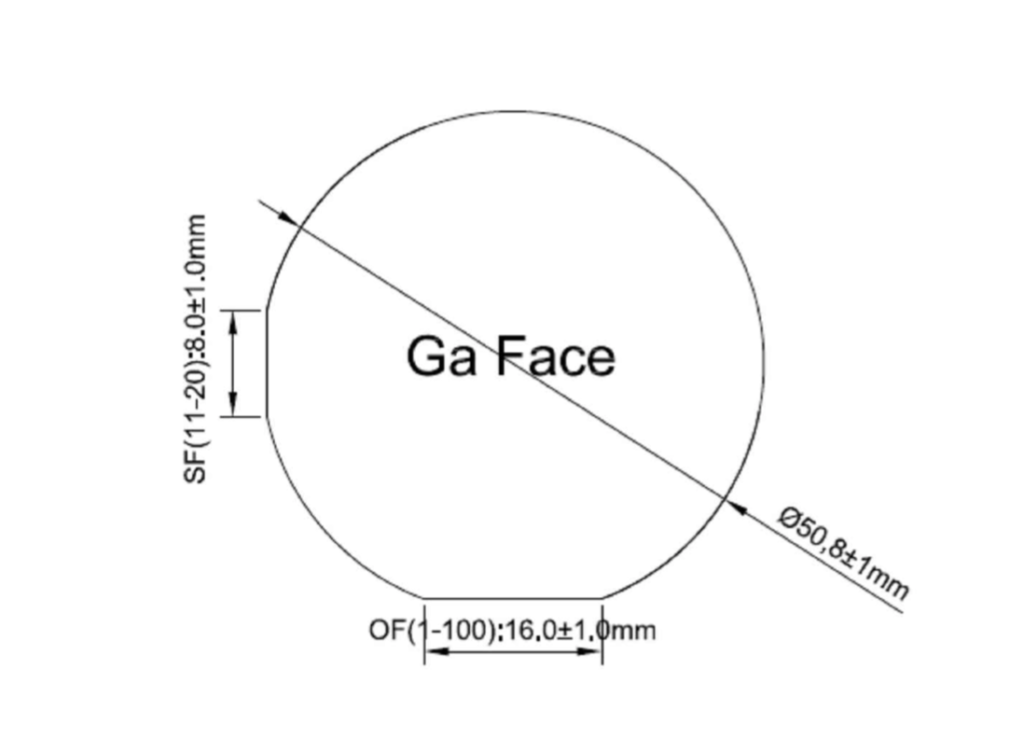
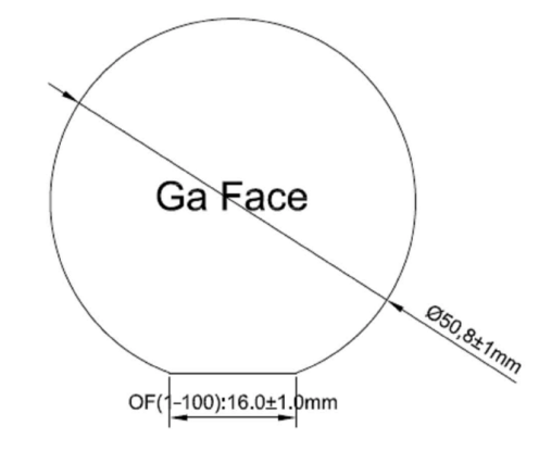
2 inch Free-Standing GaN Wafer
| Model | GaN-FS-N | GaN-FS-SI |
| Dimensions | Φ50.8mm±1mm | |
| Marco Defect Density | A Level ≦ 2/cm2 B Level > 2/cm2 |
|
| Thickness | 350± 25um | |
| Orientation | C-axis (0001)±0.5° | |
| Orientation Flat | (1-100)±0.5°,16.0±1.0mm | |
| Secondary Orientation Flat | (11-20)±3°, 8.0±1.0mm | |
| TTV (Total Thickness Variation) | ≦15um | |
| BOW | ≦20um | |
| Conduction Type | N-Type | Semi-Insulating |
| Resistivity (300K) | <0.5Ω·cm | >106Ω·cm |
| Dislocation Density | Less than 5 x 106 cm-2 | |
| Usable Surface Area | > 90% | |
| Polishing | Front Surface : Ra <0.2 nm . Epi-ready polished Back Surface : Fine ground |
|
| Package | Packaged in a class 100 clean room environment ,in single wafer containers ,under a nitrogen atmosphere. | |
| Model | GaN-FS-a | GaN-FS-m |
| Dimensions | Φ50.8mm±1mm | |
| Thickness | 350± 25um | |
| Orientation | a-plane ± 1° | m-plane ± 1° |
| TTV (Total Thickness Variation) | ≦15um | |
| BOW | ≦20um | |
| Conduction Type | N-Type | |
| Resistivity (300K) | <0.5Ω·cm | |
| Dislocation Density | Less than 5 x 106 cm-2 | |
| Usable Surface Area | > 90% | |
| Polishing | Front Surface : Ra <0.2 nm. Epi-ready polished Back Surface : Fine ground |
|
| Package | Packaged in a class 100 clean room environment, in single wafer containers, under a nitrogen atmosphere. | |
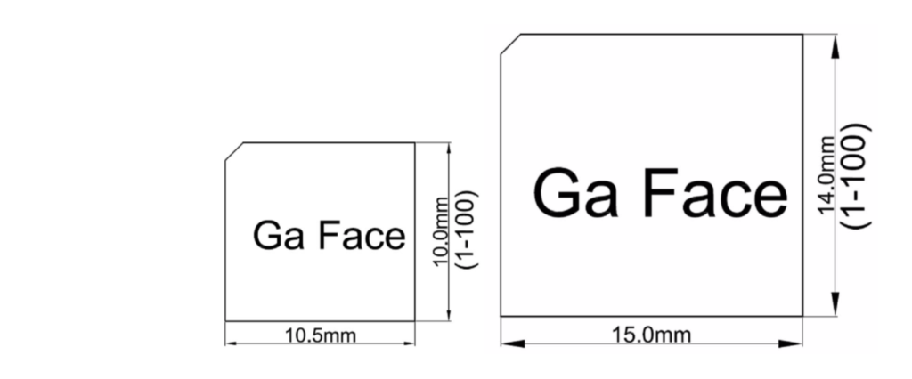
Customized Size Free-Standing GaN Substrate
| Model | GaN-FS-10 | GaN-FS-15 |
| Dimensions | 10.0mm x 10.5mm | 14.0mm x 15.0mm |
| Marco Defect Density |
A Level ≦ 2/cm2 B Level > 2/cm2 |
|
| Thickness | 300, 350, 400 ± 25um | |
| Orientation | C-axis (0001) ± 0.5° | |
| TTV (Total Thickness Variation) | ≦ 15um | |
| BOW | ≦ 20um | |
| Conduction Type | N-Type | Semi-Insulating |
| Resistivity (300K) | < 0.5Ω·cm | > 106Ω·cm |
| Dislocation Density | Less than 5 x 106 cm-2 | |
| Usable Surface Area | > 90% | |
| Polishing | Front Surface : Ra < 0.2 nm . Epi-ready polished Back Surface : Fine ground |
|
| Package | Packaged in a class 100 clean room environment, in single wafer containers, under a nitrogen atmosphere. | |
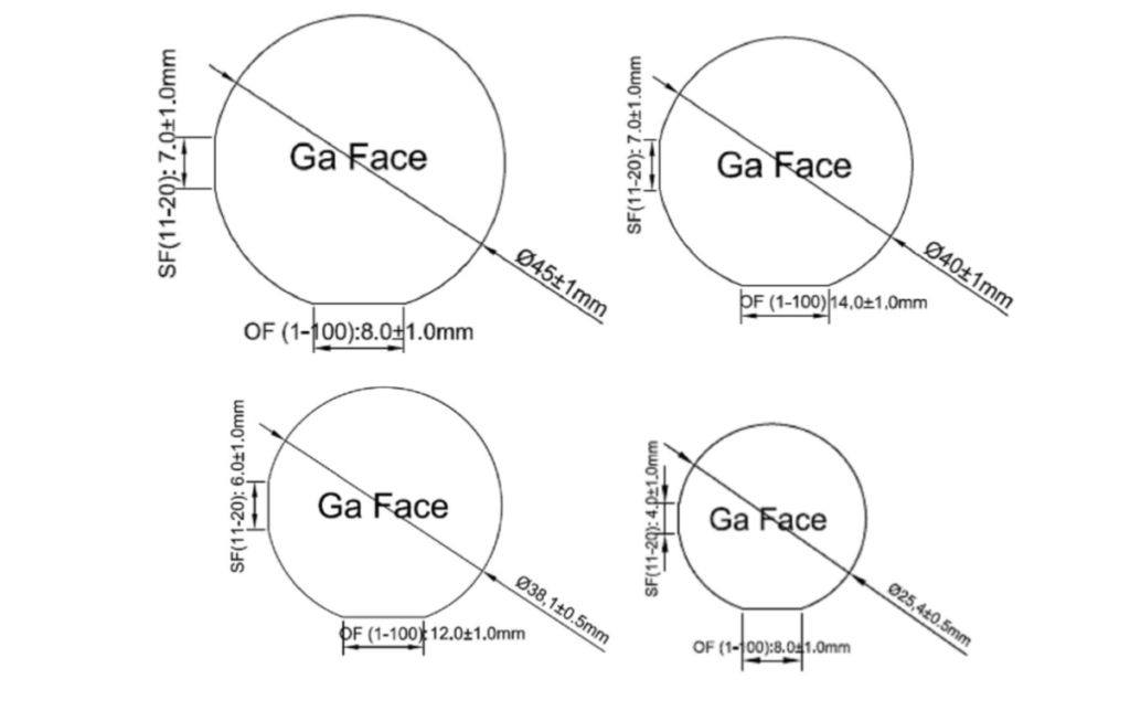
| Model | GaN-FS-Φ | |||
| Dimensions |
Φ25.4mm ± 0.5mm
|
Φ38.1mm ± 0.5mm |
Φ40.0mm ± 0.5mm
|
Φ45.0mm ± 0.5mm |
| Marco Defect Density |
A Level ≦ 2/cm2 B Level > 2/cm2 |
|||
| Thickness | 350± 25um | |||
| Orientation | C-axis (0001)±0.5° | |||
| Orientation Flat | (1-100) ± 0.5°, 8.0 ± 1mm | (1-100) ± 0.5°, 12.0 ± 1mm | (1-100) ± 0.5°, 14.0 ± 1mm | (1-100) ± 0.5°, 14.0 ± 1mm |
| Secondary Orientation Flat | (11-20)±3°, 4.0±1.0mm | (11-20) ± 3°, 6.0 ± 1mm | (11-20) ± 3°, 7.0 ± 1mm | (11-20) ± 3°, 7.0 ± 1mm |
| TTV (Total Thickness Variation ) | ≦15um | |||
| BOW | ≦20um | |||
| Conduction Type | N-Type |
Semi-Insulating |
||
| Resistivity (300K) | <0.5Ω·cm | >106Ω·cm | ||
| Dislocation Density | Less than 5 x 106 cm-2 | |||
| Usable Surface Area | > 90% | |||
| Polishing | Front Surface : Ra <0.2 nm . Epi-ready polished
Back Surface : Fine ground |
|||
| Package | Packaged in a class 100 clean room environment, in single wafer containers, under a nitrogen atmosphere. | |||
2 inch GaN Thick Film on Sapphire Wafer
| Model | GaN-T-N | GaN-T-S |
| Dimensions | Φ2 inch | |
| Thickness | 15, 20, 30, 40um | 30, 90um |
| Orientation | C-axis (0001)±1° | |
| Conduction Type | N-Type | Semi-Insulating |
| Resistivity (300K) | <0.5Ω·cm | >106Ω·cm |
| Dislocation Density | Less than 5 x 106 cm-2 | |
| Usable Surface Area | > 90% | |
| Substrate structure | GaN thick film on Sapphire (0001) | |
| Polishing |
Standard : SSP Option : DSP |
|
| Package | Packaged in a class 100 clean room environment, in single wafer containers, under a nitrogen atmosphere. | |
For inquiry, please give us the following information:
- Size with tolerance (Diameter / Thickness )
- Type
- Orientation
- Electrical resistivity
- Polishing Side (SSP or DSP )
- Quantity