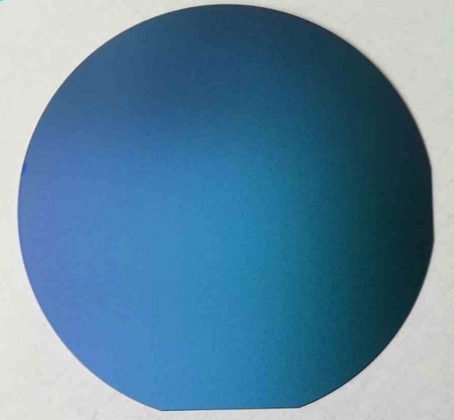
Pt/Ti/SiO₂/Si wafer
Pt(111)/Ti/SiO₂/Si wafers are multilayer substrates that offer excellent electrical conductivity and stability. The platinum (Pt) layer provides a highly conductive surface, while the titanium (Ti) layer improves adhesion between the platinum and the underlying SiO₂/Si structure. These wafers are widely used in microelectronics, MEMS (Micro-Electro-Mechanical Systems), and sensor applications, particularly where high-temperature stability and strong electrical properties are required.
For inquiry, please give us the following information:
- Size with tolerance (Diameter /layer thickness)
- Wafer type (N or P), orientation, thickness
- Polishing Side (SSP or DSP )
- Quantity
Typical Properties
| Size | 2″, 3″, 4″ | |
| Layer thickness | Pt: 100 nm, Ti: 10 nm, SiO2: 300 nm (approximately) | |
| Si wafer | P-type <100> | |
| Surface: | One side polished | |

