
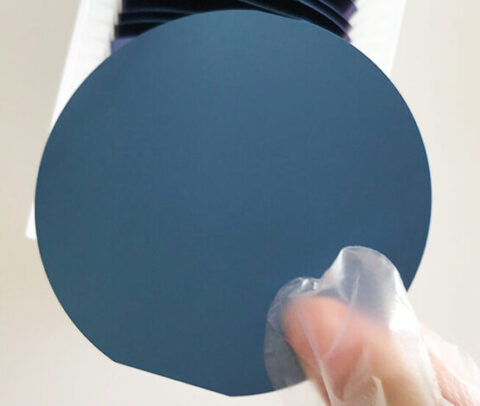
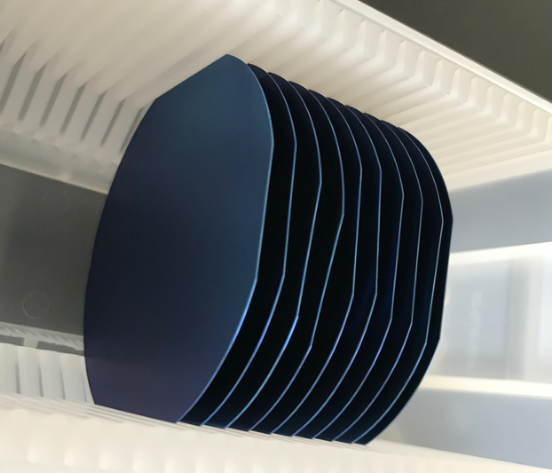
Thermal Oxide Wafer
The silicon dioxide layer forms on the wafer during thermal oxidation, a process typically carried out in a horizontal tube furnace at temperatures between 900 to 1200°C, using either wet or dry methods. This oxide layer, grown directly on the wafer, offers superior uniformity and dielectric strength compared to layers deposited by CVD. It acts as a dielectric insulator, essential for most silicon-based devices, providing surface smoothing, acting as a doping barrier, and serving as surface dielectric protection. Thermal oxidation wafers are used as substrates for various applications, including PVD/CVD coatings, magnetron sputtering, molecular beam epitaxy, and analytical techniques such as XRD, SEM, AFM.
- Size with tolerance (Diameter / Thickness /oxidation layer thickness )
- Type ( N or P type )
- Orientation
- Electrical resistivity
- Polishing Side (SSP or DSP )
- Quantity
Specifications
| Production Method | LPCVD |
| Surface Polishing | SSP/DSP |
| Diameter | 2inch / 3inch /4inch / 5inch/ 6inch |
| Type | P type / N type |
| Oxidation Layer thickness | 100nm ~1000nm |
| Orientation | <100> <111> |
| Electrical resistivity | 0.001-25000(Ω•cm) |