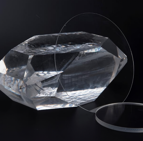
Crystal Quartz wafer
Quartz crystal wafers are precision-cut slices of monocrystalline quartz (SiO₂), known for their piezoelectricity, high mechanical and chemical stability, and high Q factor at resonance. These wafers are essential in frequency control and timing applications, commonly used in oscillators, resonators, and filters. They can be cut in different orientations, such as X-Cut, Y-Cut, AT-Cut, and ST-Cut, to optimize frequency stability and temperature performance. With the rise of MEMS and NEMS technologies, quartz crystal wafers continue to play a crucial role in advancing modern electronics.
For inquiry, please give us the following information:
- Size (Diameter/Length/Width/ Thickness)
- Cutting Angle
- Polishing Side (SSP or DSP )
- Quantity
Specifications
| Material | Quartz Crystal | |||
| Cutting Angle | X/Y/Z/AT32、33、36/BT/ST42.75°-cut etc | |||
| Diameter/size | 3”(76.2mm) | 4” (100mm) | 6″(150mm) | 8″(200mm) |
| Tol(±) | <0.20 mm | |||
| Thinnest Thickness | 0.08mm Min | 0.10mm Min | 0.20mm Min | 0.35mm or more |
| Primary Flat | 22mm | 32mm | 42.5mm | 57.5mm |
| LTV (5mmx5mm) | <1µm | |||
| TTV | <3µm | |||
| Bow | -30<bow<30 | |||
| Warp | <40µm | |||
| PLTV(<0.5um) | ≥95%(5mm*5mm) | |||
| Orientation Flat | All available | |||
| Surface Type | Single Side Polished /Double Sides Polished | |||
| Polished side Ra | <0.5nm | |||
| Back Side Criteria | General is 0.2-0.5µm or as customized | |||
| Edge Criteria | R=0.2mm or Bullnose | |||
| Material Property | ECD | Better than grade 4 | ||
| Inclusion | Better than grade II | |||
| Q-Value | Better than grade C | |||
| Wafer Surface Criteria | Particles ¢>0.3 µ m | <= 30 | ||
| Scratch , Chipping | None | |||
| Defect | No edge cracks, scratches, saw marks, stains | |||
| Packaging | Qty/Wafer box | 25pcs per box | ||

