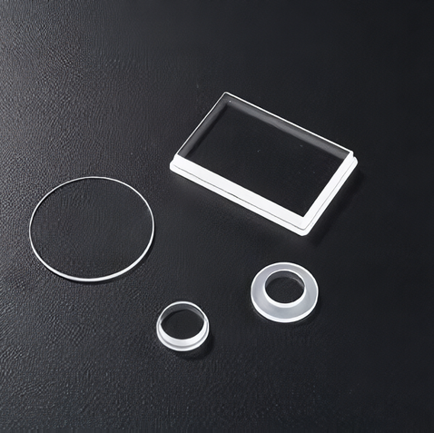
Sapphire wafer
Sapphire wafers are widely used in electronics and optics due to their exceptional hardness, high thermal conductivity, and excellent optical transparency. They are highly resistant to chemical and thermal damage, making them ideal for use in harsh environments. Common applications include LED production, optical windows, and substrates for semiconductor devices. Sapphire’s transparency across a broad range of wavelengths also makes it valuable in laser and infrared systems.
For inquiry, please give us the following information:
- Size with tolerance (Diameter /Thickness)
- Primary flat
- Polishing Side (SSP or DSP )
- Quantity
Specifications
| 2 inch | 3 inch | 4 inch | 6 inch | 8 inch | 12 inch | |
|---|---|---|---|---|---|---|
| Diameter | 50.8 ± 0.1 mm | 76.2 ± 0.1 mm | 100 ± 0.1 mm | 150 ± 0.1 mm | 200 ± 0.1 mm | 300 ± 0.1 mm |
| Thickness | 100 ± 15 µm 430 ± 15 µm 500 ± 15 µm |
100 ± 15 µm 430 ± 15 µm 500 ± 15 µm |
200 ± 15 µm 500 ± 15 µm 650 ± 15 µm |
350 ± 15 µm 500 ± 15 µm 1000 ± 15 µm |
700 ± 25 µm 1000 ± 25 µm or customized |
725 ± 25 µm 1600 ± 25 µm or customized |
| Roughness | Ra ≤ 0.2 nm | Ra ≤ 0.2 nm | Ra ≤ 0.2 nm | Ra ≤ 0.2 nm | Ra ≤ 0.3 nm | Ra ≤ 0.5 nm |
| Warp | ≤ 10 µm | ≤ 10 µm | ≤ 10 µm | ≤ 15 µm | ≤ 30 µm | ≤ 60 µm |
| TTV | ≤ 3 µm | ≤ 10 µm | ≤ 10 µm | ≤ 10 µm | ≤ 10 µm | ≤ 10 µm |
| Scratch/Dig | 20/10 | 20/10 | 20/10 | 20/10 | 40/20 | 60/40 |
| Polish | SSP (Single Side Polished) or DSP (Double Side Polished) | |||||
| Primary flat | 16 mm | 22 mm | 32.5 mm | 47.5 mm | NOTCH | NOTCH |
| Edge Form | 45° Shape | |||||
Specifications
| 2 inch | 3 inch | 4 inch | 6 inch | 8 inch | 12 inch | |
| Diameter | 50.8 ± 0.1 mm | 76.2 ± 0.1 mm | 100 ± 0.1 mm | 150 ± 0.1 mm | 200 ± 0.1 mm | 300 ± 0.1 mm |
| Thickness | 100 ± 15 µm 430 ± 15 µm 500 ± 15 µm |
100 ± 15 µm 430 ± 15 µm 500 ± 15 µm |
200 ± 15 µm 500 ± 15 µm 650 ± 15 µm |
350 ± 15 µm 500 ± 15 µm 1000 ± 15 µm |
700 ± 25 µm 1000 ± 25 µm or customized |
725 ± 25 µm 1600 ± 25 µm or customized |
| Roughness | Ra ≤ 0.2 nm | Ra ≤ 0.2 nm | Ra ≤ 0.2 nm | Ra ≤ 0.2 nm | Ra ≤ 0.3 nm | Ra ≤ 0.5 nm |
| Warp | ≤ 10 µm | ≤ 10 µm | ≤ 10 µm | ≤ 15 µm | ≤ 30 µm | ≤ 60 µm |
| TTV | ≤ 3 µm | ≤ 10 µm | ≤ 10 µm | ≤ 10 µm | ≤ 10 µm | ≤ 10 µm |
| Scratch/Dig | 20/10 | 20/10 | 20/10 | 20/10 | 40/20 | 60/40 |
| Polish | SSP (Single Side Polished) or DSP (Double Side Polished) | |||||
| Primary flat | 16 mm | 22 mm | 32.5 mm | 47.5 mm | NOTCH | NOTCH |
| Edge Form | 45° Shape | |||||

