
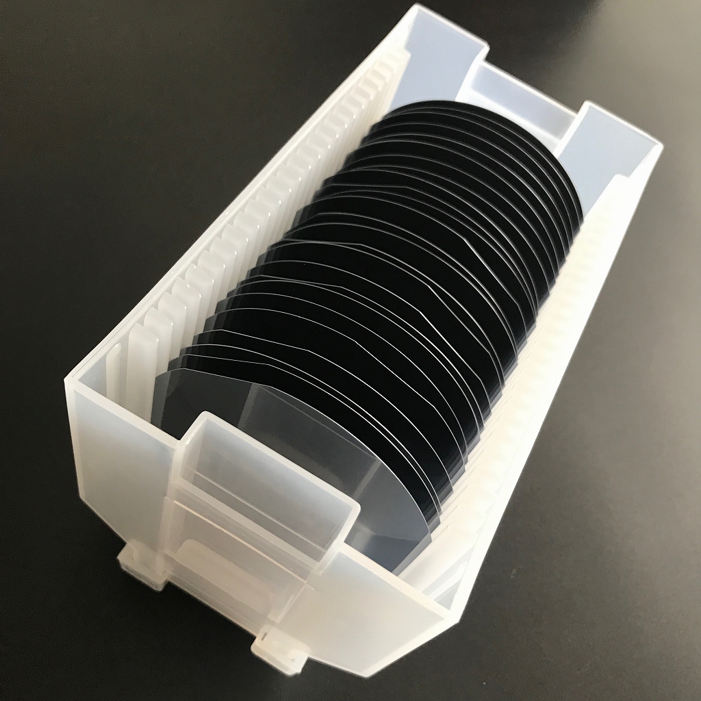
Silicon wafers
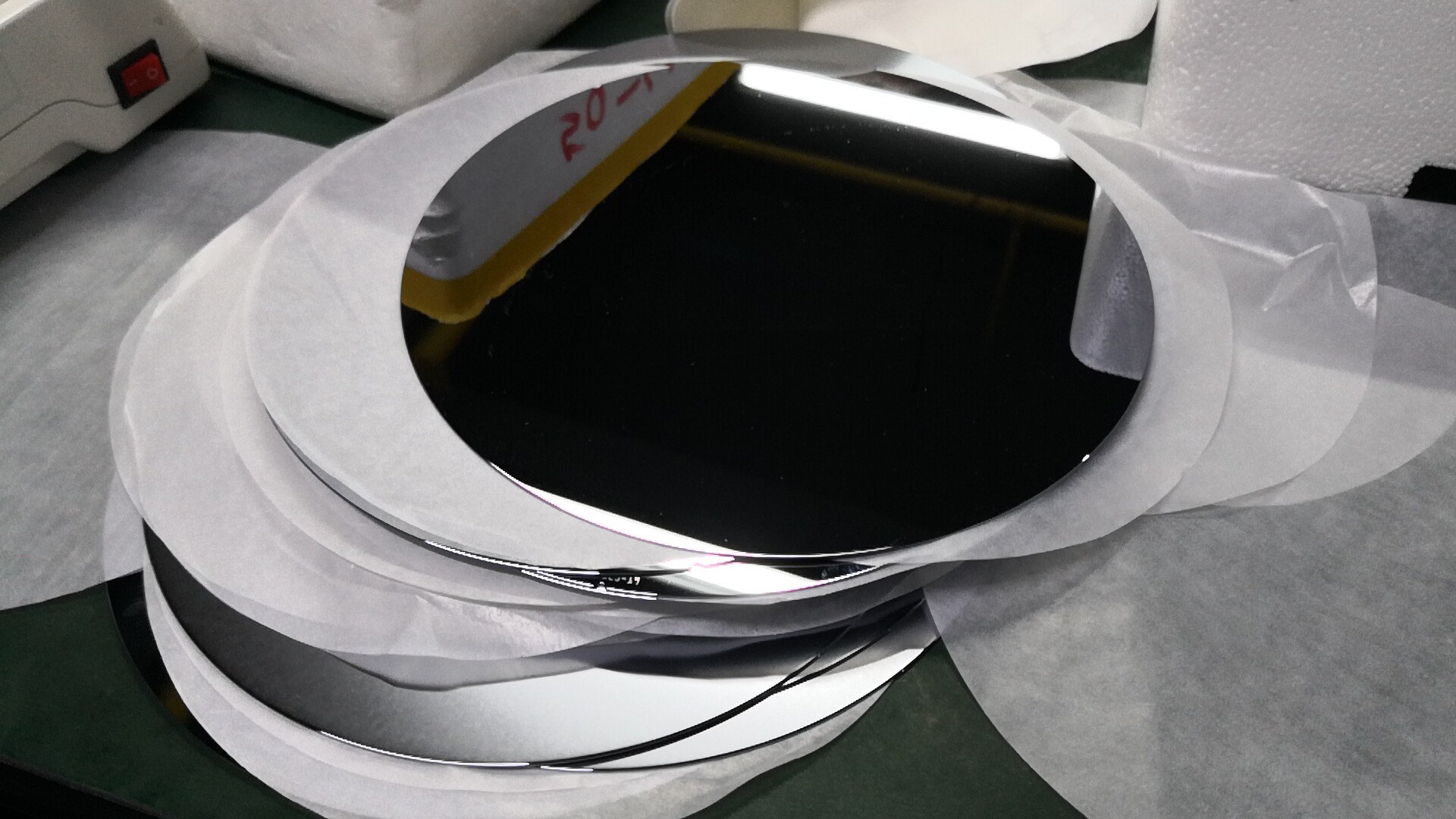
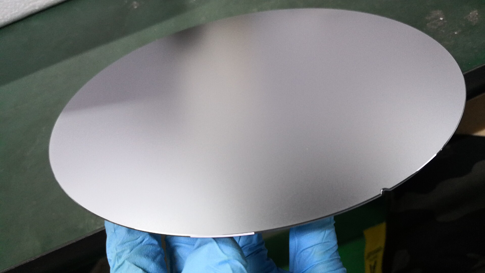
Silicon (Si) wafers are highly versatile substrates widely used in various scientific and industrial applications due to their excellent mechanical and electrical properties. Key features of Si wafers include high purity, flatness, and smooth surface, making them ideal for high-precision experiments and semiconductor device fabrication.
Applications include their use as a carrier for synchrotron radiation samples, substrates for PVD/CVD coatings, and growth samples for magnetron sputtering. Si wafers are also employed in XRD, SEM, and Atomic Force Microscopy (AFM), as well as infrared and fluorescence spectroscopy. Additionally, they serve as substrates for molecular beam epitaxial growth and X-ray analysis of crystalline semiconductors.
For inquiry, please give us the following information:
- Size with tolerance (Diameter /Thickness)
- Type (N or P)
- Orientation
- Primary flat
- Polishing Side (SSP or DSP )
- Quantity
Specifications
| Production Method | CZ |
| Diameter | 2 inch / 3 inch / 4 inch / 6 inch / 8 inch |
| Thickness | 100 µm, 200 µm, 300 µm, 400 µm, 500 µm, 600 µm, 700 µm, 800 µm, 900 µm, 1000 µm |
| Type | N type / P type |
| Orientation | <111>, <100>, <110> |
| Resistivity | 0.002 ~ 25000 Ω.cm |
| Flatness TIR | < 3 µm |
| Warping degree TTV | < 10 µm |
| Flexibility BOW | < 10 µm |
| Roughness | < 0.5 nm |
| Granularity | < 10 (for size > 0.3 µm) |